Direkt zum Hauptinhalt
Suchbegriff eingeben
Suche und Suchergebnis
Service-Navigation
Start
Fachbereiche
01
Rechtswissenschaften
02
Wirtschaftswissenschaften
03
Gesellschaftswissenschaften und Philosophie
04
Psychologie
05
Evangelische Theologie
06
Geschichte und Kulturwissenschaften
09
Germanistik und Kunstwissenschaften
10
Fremdsprachliche Philologien
12
Mathematik und Informatik
13
Physik
15
Chemie
16
Pharmazie
17
Biologie
19
Geographie
20
Medizin
21
Erziehungswissenschaften
Alle Einrichtungen
Portale
Alumni-Portal
Forschungsinformationssystem
Hochschulrechenzentrum
ILIAS
Karriere
Katalog Plus
Marvin
Personensuche
Universitätsbibliothek
Vorlesungsverzeichnis
Webmail Beschäftigte
Webmail Studierende
Zeiterfassung
English
high-contrast version
Suche und Suchergebnis
Haupt-Navigation
Philipps-Universität Marburg - Startseite
Studium
Bereich
Studium
Inhalte
Vor dem Studium
Im Studium
Nach dem Abschluss
Beratung & Service
Schnellzugriff
Studienangebot
Semestertermine
Bewerben und Einschreiben
Start ins Studium
Anträge und Formulare
FAQ
Forschung
Bereich
Forschung
Inhalte
Forschungsprofil
Spitzenförderung
Junge Talente
Forschungsförderung
Kontakt & Service
Schnellzugriff
Exzellenzstrategie
Sonderforschungsbereiche
EU-Förderung
Transferabteilung
Promovieren in Marburg
Forschungsdatenmanagement
Transfer
Bereich
Transfer
Inhalte
Transfer@UMR
Wissen entdecken
Zukunft gestalten
Wissenschaft fördern
Kontakt
Schnellzugriff
Kooperationen
Fundraising & Alumni-Service
Veranstaltungen
Gast- und Seniorenstudium
Studentisches Engagement
Fördernde
International
Bereich
International
Inhalte
Aus dem Ausland
Ins Ausland
Internationales Profil
Service intern
Kontakt & Service
Schnellzugriff
Welcome & Support Services
Förderprogramme
EUPeace
Mobility-Online
Lagepläne
Universität
Bereich
Universität
Inhalte
Profil
Administration
Einrichtungen
Lehre
Presse & Kommunikation
Service & Beratung
Schnellzugriff
Personal
Karriere
Formular-Center
Sicherheit
Lagepläne
Kontakt
Mobile-Navigation
Suchbegriff eingeben
Hauptmenü öffnen
Universität Marburg
schließen
Zurück
Home
Fachbereiche
Portale
English
Fachbereiche
zurück
01
Rechtswissenschaften
02
Wirtschaftswissenschaften
03
Gesellschaftswissenschaften und Philosophie
04
Psychologie
05
Evangelische Theologie
06
Geschichte und Kulturwissenschaften
09
Germanistik und Kunstwissenschaften
10
Fremdsprachliche Philologien
12
Mathematik und Informatik
13
Physik
15
Chemie
16
Pharmazie
17
Biologie
19
Geographie
20
Medizin
21
Erziehungswissenschaften
Alle Einrichtungen
Portale
zurück
Alumni-Portal
Forschungsinformationssystem
Hochschulrechenzentrum
ILIAS
Karriere
Katalog Plus
Marvin
Personensuche
Universitätsbibliothek
Vorlesungsverzeichnis
Webmail Beschäftigte
Webmail Studierende
Zeiterfassung
Suche
Kontrastreiche Version
Philipps-Universität Marburg - Startseite
mar.quest
Marburg Center for Quantum Materials and Sustainable Technologies
Fachbereichs-Navigation
Marburg Center for Quantum Materials and Sustainable Technologies
Zentrum
Motivation
Ausschreibungen
Direktorium
Forschung
Schwerpunkte
Arbeitsgruppen
Forschungsverbünde
Gerätezentren
Elektronenmikroskopie und Rastersonden-Methoden
Halbleiterepitaxie
PeroLab
Optische Spektroskopie
PhD School
Struktur
Events
Aktuelles Semester
Vergangene Semester
nach oben scrollen
mar.quest | Marburg Center for Quantum Materials and Sustainable Technologies
mar.quest | Marburg Center for Quantum Materials and Sustainable Technologies
Fachbereichs-Navigation
mar.quest | Marburg Center for Quantum Materials and Sustainable Technologies
schließen
Zurück
Startseite
Hauptinhalt
Philipps-Universität Marburg - Marburg Center for Quantum Materials and Sustainable Technologies
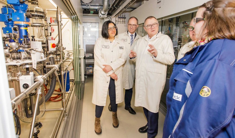
Foto: HA Hessen Agentur GmbH – Jan Michael Hosan
Willkommen auf den Seiten des Marburg Center for Quantum Materials and Sustainable Technologies (mar.quest)
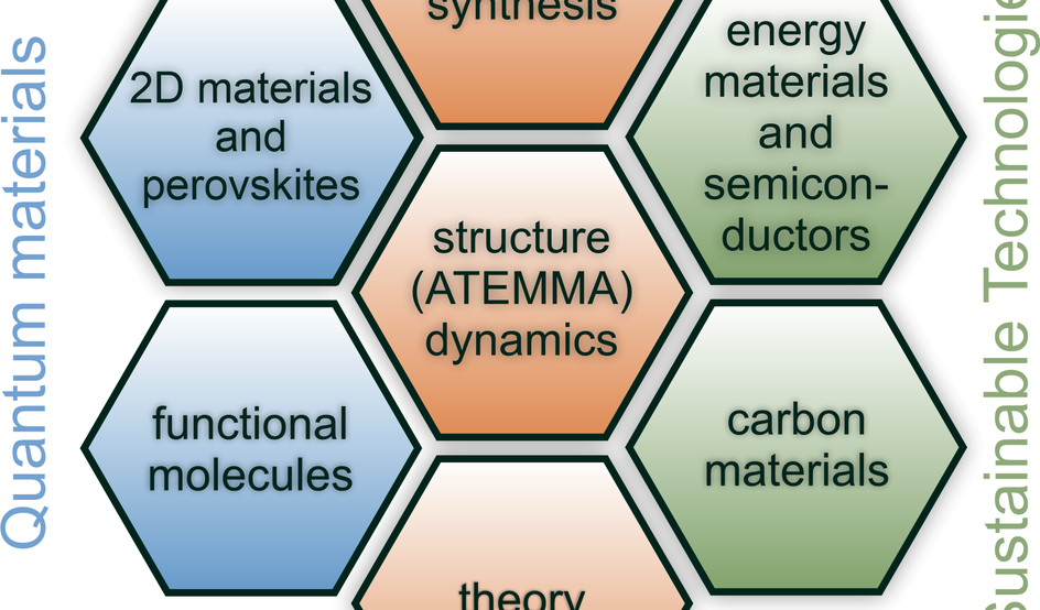
Inhaltliche Ausrichtung
Themen
Zentrum
Forschung
Gerätezentren
Übersicht über die Gerätezentren von mar.quest
PhD School
PhD School (Graduiertenschule) von mar.quest
Events
Zurückblättern
Vorblättern
Zentrum
Forschung
Gerätezentren
Übersicht über die Gerätezentren von mar.quest
PhD School
PhD School (Graduiertenschule) von mar.quest
Events
Aktuelles
Nachrichten
16.03.2026
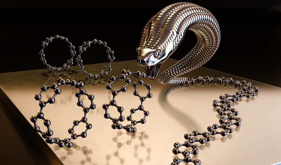
Molekülketten mit Biss: Team aus Marburg und Gießen erzielt Durchbruch in der Polymerforschung
13.02.2026
Marburger Hightech-Forschung erhält 500.000 Euro LOEWE-Förderung
12.02.2026
Neue Arbeitsgruppe erforscht Solarzellen der Zukunft
05.02.2026
Neues Licht auf Ladungstransfer in organischen Halbleitern
16.01.2026
Solarenergie im Terawatt-Maßstab: Nachhaltigkeit entscheidet sich heute
Alle Nachrichten
Zurückblättern
Vorblättern