Main Content
Spectroscopy on new materials and nanophotonics
The research of new materials like graphene and mono-layer two-dimensional (2D) semiconductor materials and insulators has become the international focus of attention of current research, because of their novelty and their exceptional properties. The class of sub-nanometer 2D materials, which may be used in future optoelectronic components, is increasingly researched in Marburg by material scientists and physicists. After the first successful investigations and publications and in conjunction with micro- and nano-structures the unique optoelectric properties of these materials are supposed to allow the creation of innovative nano-lasers, photo-detectors, and functionalized boundary-systems.
Hereafter, examples shall provide an impression of new interesting materials, nanostructures, and components.
With nano-structures to more efficient detection of light
To combine nano-particles and two-dimensional materials in innovative photo-detector structures was the objective of our bi-national team of physicists of the Zhejiang-University in Hangzhou, China, and the Philipps-University Marburg. In our recent studies we pursue mainly simple but at the same time playful and scientifically exciting approaches in order to implement interesting concepts.
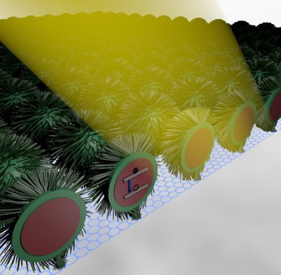
Figure 2: Schematics of a one-atom layer of graphene, which was functionalized by applied quantum dots to absorb light efficiently in order to provide a light detecting device.
We have examined our special photo-detector eventually with regard to an improvement of the light detection via an electric back-contact voltage in Marburg in the semiconductor photonics research group of Prof. Martin Koch and the research group of Prof. Heimbrodt. The main objective was to characterize the transfer of light created charge carriers, respectively energy from the quantum dots to the graphene with a suitable system of quantum dots and graphene transistors.
One study presents, for example, a self-created graphene field-effect transistor, build with laser processing and electric contacting, which uses the special electric properties of the ultra-thin layer of carbon, the so-called graphene, and the high efficient light absorption of nano-sized semiconductor particle, the colloidal quantum dots. This increasingly examined components of the research can be created relatively easily and also be bought without complications. They are supposed to be used in more and more applications like lighting, display technology, photovoltaic and light detection.
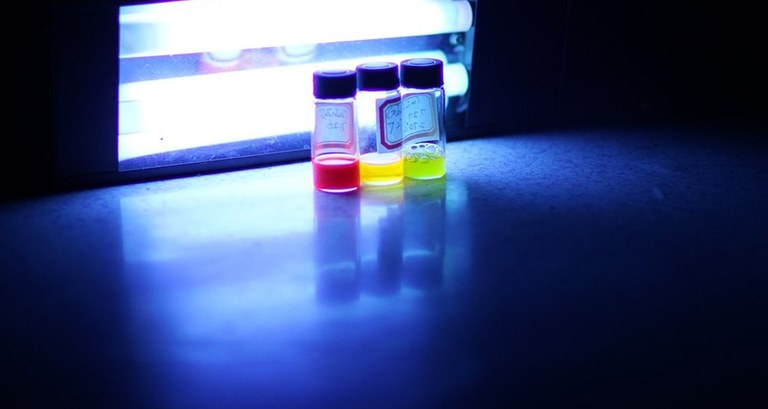
Figure 3: Quantum dots in solution.
Our team researches the physic of inner boundaries intensively within the framework of a collaborative research center (CRC) (SFB 1083). The mechanism and efficiency of charge transfer are dependent on the properties of the boundary between quantum dots and graphene. We could influence the properties of nanoparticles in solution and the distance to the graphene and its way of interaction with the graphene by choosing suitable coatings for the quantum dots. Thereby we could achieve a change in the energy transfer rate via change of transistor voltage and measure the effect with optical spectroscopy. Thus we could find the best operating point for this photodetector and adjust it accordingly. The examined behavior is in good accordance with a theoretical "Förster-Resonance" energy transfer model. Currently, we plan to conduct examinations with different materials and improved structures.
Our research in this field was supported by the Philipps-Universität Marburg, the Deutsche Forschungsgemeinschaft (DFG: SFB 1083), the Bundesministerium für Bildung und Forschung (BMBF) within the context of the program for the strategic partnership of the Deutschen Akademischen Austauschdienst (DAAD) and the National Natural Science Foundation of China. This successful collaboration in the field of quantum dot graphene photodetectors was possible due to the skillful use of common competencies of both universities in the fields of semiconductor spectroscopy and material science and both way visits of project coordinators and students. It is a great opportunity for our students to participate in current research in an expert team abroad.
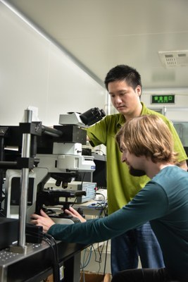
Figure 4: Maximilian Schneider (front) and Ruifeng Li together in the laboratory at Zhejiang-University, Hangzhou, in China.
Further information:
Original publication: Ruifeng Li, Lorenz Maximilian Schneider et al: Gate Tuning of Förster Resonance Energy Transfer in a Graphene - Quantum Dot FET Photo-Detector, Scientific Reports 6:28224 (2016), www.nature.com/articles/srep28224
Contact: Dr. Arash Rahimi-Iman