Main Content
(Nano)structure and characterization facilities
Transmission electron microscopy (TEM)
Coming soon
ATEMMA
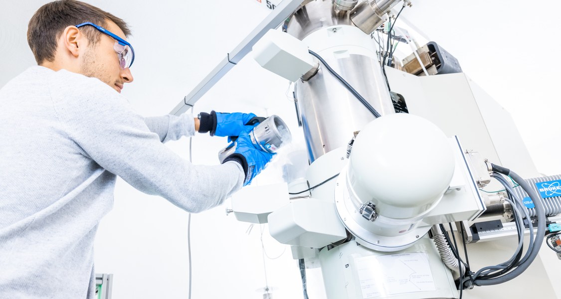
Double Cs-corrected TEM JEM 2200FS
- high tension: 80 and 200 kV
- Cs-correctors (CEOS) for the probe forming as well as imaging system
- in-column energy filter
- energy dispersive X-ray detector (Bruker)
- two high angle annular dark field detectors
- bright field detector
- 4k x 4k camera (TVIPS XF416)
- fast 2k x 2k camera (Ultrascan Gatan)
- pixelated detector (PNDetector)
- analytical double tilt sample holder (JEOL)
- liquid nitrogen sample holder (Gatan)
- electrothermal sample holder (Protochips Fusion)
- tomography holder (Fischione)
- gas cell (Protochips Atmosphere)
- liquid cell (Protochips Poseidon)
- inert gas / vacuum transfer holder (Melbuild)
- precession diffraction system (NanoMegas)
TEM JEM 3010
- high tension: 100 ... 300 kV
- ultra-high resolution pole piece
- 4k x 4k camera (TVIPS XF416)
- precession diffraction system (NanoMegas)
Image simulations
- STEMsalabim
- JEMS
- HREM for reconstruction of exit wave function amplitude and phase
- HREM for Z-contrast imaging simulation (absorptive potential method)
- geometric phase analysis
- peak pair analysis
TEM sample preparation
- polishing (Multiprep Allied)
- dimpling (Fischione)
- ion milling (PIPS Gatan)
- gentle milling (Nanomill Fischione)
- plama cleaning (Fischione)
- cryo-microtom (Leica)
Further Electron Microscopes and sample preparation equipment can be found here.
Focussed Ion Beam and Scanning Electron Microscopy
Helios 5 Hydra CX PFIB - Dual-Beam Analytical SEM and Plasma FIB
- electron gun with hot field emitter cathode
- focussed ion gun
- four gas plasma sources (Xe, Ar, O, N)
- ToFWerk Time-of-flight secondary ion mass spectrometer (SIMS)
- EDX
- Cryostage
- inert and vacuum gas transfer (clean connect)
- hight current processing (60 nA - 200 nA) with protective shutter
- stage bias and beam deceleration up to 4000 V
- charge neutralizer (flood gun)
- oxygen plasma cleaner
- carbon, platin and tungsten gas injection
JEOL JIB 4610F, dual beam FIB/SEM
- thermal field emission gun (Schottky)
- gallium ion source
- carbon and tungsten gas injection systems
- backscattered and secondary electron detector
- micro manipulator (Kleindiek)
- microgripper (Kleindiek)
- EDX detector, Bruker XFlash 5010, 10 mm2 active area
- electron backscatter detection (EBSD, Bruker)
SEM Hitachi cold field emission gun
- high tension: 5 ... 30 kV
- secondary electron detector
- backscattered electron detector
- energy dispersive X-ray analysis (EDX) (Oxford)
- electron beam induced current (EBIC)
Atomic force microscopy (AFM)
- Digital Instruments Nanoscope IIIa
X-ray diffraction
- high resolution optics
- open detector
- reciprocal space mapping
- GIXS (gracing incidence X-ray scattering)
- XRR (X-ray reflectivity)
Photoluminescence (PL)
- Ar-ion laser
- excitation spectroscopy
- absorption spectroscopy
- photo-current spectroscopy
- reflection spectroscopy
- 5 - 350 K
- laser diode measurement
- wafer PL and reflectivity mapping (accent mapper; solid state lasers @ 532 and 980 nm)
Magnetotransport/Hall
- Hall, conductivity
- 0 - 0.8 T
- 10 - 500 K