Main Content
Research
The manifold properties of conducting and semiconducting organic molecules have already enabled a number of novel technical applications like highly efficient displays employed in mobile devices (e.g. AMOLED displays) or organic solar cells. However, the comprehension of numerous fundamental physical processes in such materials and especially multilayered devices is still insufficient. To bridge this gap and help develop an extensive understanding of these systems our research group prepares suitable model systems of organic semiconductors of which analysis potentially allows to address and understand such physical processes.
In particular, these topics comprise our main research interests:
- Preparation of well-defined model systems of organic semiconductors
- Correlation of structural and spectroscopic properties
- Set-up and investigation of prototypical applications
Preparation of well-defined model systems of organic semiconductors
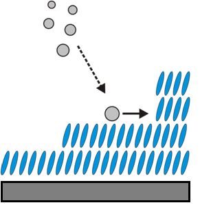
Our approach is to produce samples of high structural order and purity in order to reliably derive information on the properties of molecular solids. In order to achieve sufficient sample quality, different preparation methods are utilized for each investigated material. In our research group such samples are typically prepared either as well-defined organic thin films with typical thicknesses of 1-100 nm under ultrahigh vacuum conditions (via Organic Molecular Beam Deposition), as organic single crystals or via immersion techniques.
An important experimental step that is closely connected to the preparation process is the precise structural characterization of the processed samples. By combining different microscopic, spectroscopic and diffraction methods, both the arrangement of single molecules on surfaces and the crystallinity and molecular orientation in the molecular solids can be analyzed (further details presented in "Methods").
In many cases, the structure and morphology of molecular thin films are determined by the physical properties of the applied substrates not only in the first monolayers but also in multilayer films of comparably large film thickness. Therefore, choosing the appropriate substrate directly allows controlling the thin film properties. The global orientation of molecules, for example, can be controlled by using supporting substrates which exhibit an epitaxial relationship with the molecular compound. This is of particular interest since molecular solids often feature a strong anisotropy of their optical and electronic properties. Moreover, the reactivity of the applied substrates results in different film properties for both, monolayer and multilayer films. In particular, reactive metal surfaces such as copper or silver often induce distinctly different adsorption and growth modes than insulators such as silicon dioxide or alkali halides.
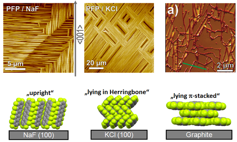
Highly ordered thin films of perfluoropentacene molecules prepared on different supporting substrates. The Atomic Force Microscope enables insight into the different surface arrangements (above), by X-ray diffraction measurements the – highly different – molecular orientations can be determined (below).
Correlation of structural and spectroscopic properties
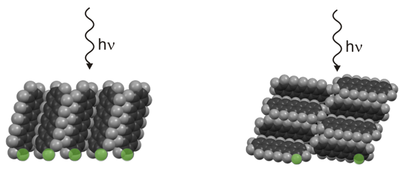
One of our significant research goals is to investigate correlations between the structural and the spectroscopic characteristics of the examined model systems with particular emphasis on the electronic properties. An exemplary question in this context is in which way electromagnetic radiation (e.g. light) interacts with molecular solids as a function of the molecular orientation. For this purpose, we perform structurally resolved spectroscopic measurements on sufficiently ordered samples. In many cases we observe that the characteristics of the molecular solids are fundamentally different from those of isolated molecules and particularly the packing motif in the solid – the relative arrangement of the molecules in the crystal unit cell – determines the spectroscopic properties. Consequently, molecular thin films can exhibit strikingly different color appearances under the polarization microscope depending on the light polarization, which may e.g. be parallel to the direction of effective molecular stacking ("parallel") or the direction where molecules are tilted to one another ("zig-zag") (more details). Even the dynamic of charge carriers in organic solar cells is crucially defined by such subtle differences in the solid structure (more details).
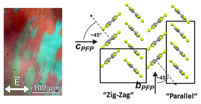
The color appearance of a molecular thin film is crucially determined by the packing motif of the molecules (schematic in top view).
Set-up and investigation of prototypical applications
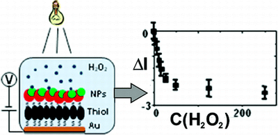
For appropriate molecular materials we use our expertise in controlling nanostructures and microscopic processes to develop prototypic applications. Besides extensive research efforts on organic field-effect transistors in the past, we participated for example in the development of a light-controlled sensor for the detection of hydrogen peroxide on the basis of self-assembled monolayers in combination with CdSe quantum dots (more details), paving the way to modern “lab-on-a-chip” applications. In a further project we have investigated the possibility to control the form and gene expression of stem cells by manipulating the cell culture substrate (more details). In the framework of a research project funded by the Deutsche Forschungsgemeinschaft (DFG) our research group is currently working on the development of novel photo-bioelectrochemical detector electrodes. In these projects, the development of prototypical applications is always closely connected to detailed structural and spectroscopic characterization to gain insights into fundamental mechanisms in this context and to verify the reliability of the realized applications.
Collaborative Research Centers
Besides a number of collaborative projects within and outside of the Philipps University Marburg our research is particularly embedded in the following Research Centers:
GRK 1782: Functionalisation of Semiconductors
The Research Training Group "Functionalization of Semiconductors" deals with the development, characterization and integration of novel materials on currently used semiconductors.
SFB 1083: Internal Interfaces
The Collaborative Research Centre SFB 1083 of the German DFG is focused on the spectroscopic and the structural analysis as well as the theoretical modelling of internal interfaces of different buried hetero-interfaces.