Main Content
Atomic Force Microscopy (AFM)
Atomic Force Microscopy is performed in different measurement modes, of which we present a selection here:
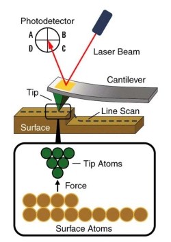
Contact-AFM
For this mode a very fine tip, which is mounted on a spring (cantilever, see right figure above), is raster-scanned over the surface of the sample. The forces occurring thereby cause the cantilever to bend. A laser beam focused on the cantilever experiences a deflection which is detected by a 4-quadrant photodiode. Line by line, a topographical image of the surface is produced (below animations of the measurement principle in Constant Height (left) and Constant Force Mode (right)).
Tapping-AFM
Since scanning in Contact Mode can damage a thin organic layer, a mode for this kind of samples is used, in which the cantilever oscillates at a frequency close to its resonance frequency. Overall, less energy is transferred the sample and the lateral resolution is higher compared to Contact Mode. Here, two modes are possible: Firstly, the cantilever can be oscillated by means of piezo elements, secondly a motion via an oscillating magnetic field is possible (Top-MAC-Mode, spool in a nosecone provided for this purpose, a magnetizable cantilever is necessary, measurements in solution are possible).
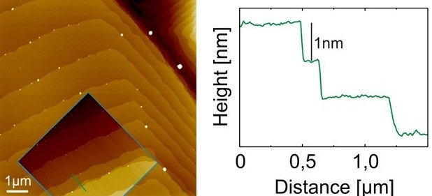
As an example, an image in Top-MAC-Mode: Pentacene on a silicon wafer, monomolecular terraces can be seen.
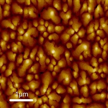
An Example for AC-Mode: Surface of a perylene crystal with monomolecular terraces
Dynamic Lateral Friction Microscopy
For this mode the cantilever is excited to oscillate in lateral direction, i.e. parallel to the surface of the sample. If there are areas on the surface of the sample with different frictional properties, the oscillation there is attenuated to different extents. Therefore, a contrast in the energy dissipation can be seen in the image of the attenuated amplitude.
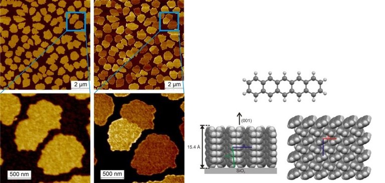
Example DLFM: Pentacene submonolayer on SiO2. Left: Topography with the same height of the islands; DLFM amplitude with contrast between pentacene domains relatively rotated towards each other, note the domain boundaries. Right: Schematic of the structure of a pentacene monlayer on SiO2. The frictional properties differ in a- and b-direction, which results in the formation of the shown DLFM contrasts.
Current Sensing
A voltage can be applied between sample and tip. Thus, in Contact-Mode, in addition to the topography, the electric current can be displayed.
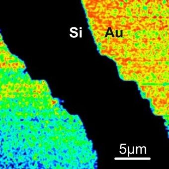
Example Current Sensing: Scratches in a polycrystalline Au layer on Si.
For these measurements in controlled atmosphere and controlled gas environment our research group uses an Agilent 5500 SPM. Furthermore, a microscope integrated into a UHV system is available.