Main Content
Low-Energy Electron Diffraction (LEED)
LEED is a diffraction technique which utilizes a beam of low energy electrons (30-250 eV) and is widely used as a standard technique to check the crystallographic quality of a surface (either clean surfaces or surfaces with ordered adsorbate overlayers). Due to the small inelastic mean free path of only a few Angstrom (typically less than 10 Å) electrons in this energy range sample only the top most atomic layers of a surface and are, therefore, well suited to analyze surface geometries. In the experiment (see Figure 1) the structural information is gained from the analysis of the angular distribution (diffraction pattern) of electrons that are elastically backscattered from the surface and detected by a fluorescent screen (see Fig. 1).
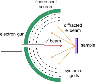
Figure 1: Schematic representation of a triple-lattice LEED setup.
The diffraction pattern is directly related to the reciprocal lattice of the sample - a lattice which represents the Fourier transform of the original lattice.
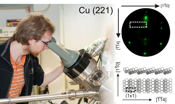
Figure 2: LEED setup and pattern of a Cu(221) surface with schematic representation of the atomic arrangement.
Typical questions addressed with this method are:
- Resulting atomic ordering of a substrate [1]:
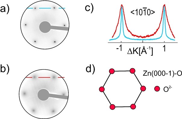
Figure 3: Comparison of LEED patterns (58 eV) of ZnO(000-1)-O-surfaces obtained after (a) heating in air and (b) UHV-based cleaning cycles, together with (c) corresponding profiles of the diffraction peaks. Schematice of the ZnO wurzite crystal structure (d) together with the top view of ideal bulk terminated ZnO surfaces of (000-1) orientation.
From the difference in sharpness of LEED-spots in this example we can clearly see the difference in atomic ordering of the O-terminated ZnO(000-1) surface produced by using various preparation procedures. The width of the diffraction spots in the Fig. 3c) reflects different degree of lateral order.
- Structural order of an absorbed thin film on a substrate [2]:
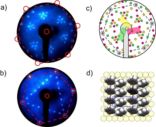
Figure 4: The measured LEED patterns with a) E = 75 eV and b) E = 99 eV of AntSe SAMs on an Au(111) surface. The reciprocal lattice c) of a (√3 × 4)rect. structure including rotational domains. Dashed red and blue hexagons in a), b) and c) respectively represent the first-order diffraction pattern of a bare Au(111) surface. d) A structural model of the AntSe SAM.
LEED patterning can be a powerful tool to ascertain the true superstructure of a self-assembled monolayer (SAM). In the shown example Anthraceneselenolate–SAMs (AntSe) form a commensurate (√3 ×4)rect. superstructure on Au(111) substrates, which, however occurs in 3 rotational domains according to the 3-fold symmetry of the substrate surface (single domains marked by colors in c). Depending on the actual electron energies various diffraction spots become visible (Fig. 4 a-b).
Some exemplary publications of our group where low-energy electron diffraction has been used:
- [1] Rapid preparation of highly ordered ultraflat ZnO surfaces.
Jan Götzen and Gregor Witte
Applied Surface Science 258 (24), 10144-10147 (2012)
Full Text - [2] Selenium as a Key Element for Highly Ordered Aromatic Self-Assembled Monolayers.
Asif Bashir, Daniel Käfer, Jan Müller, Christof Wöll, Andreas Terfort, and Gregor Witte
Angewandte Chemie Int. Ed. 47 (28), 5250-5252 (2008)
Full Text - Interface Structure and Evolution of Dinaphthothienothiophene (DNTT) Films on Noble Metal Substrates.
Maximilian Dreher, Daniel Bischof, Felix Widdascheck, Andrea Huttner, Tobias Breuer, Gregor Witte
Advanced Materials Interfaces 5 (21), 1800920 (2018)
Full Text