Main Content
Scanning Tunneling Microscopy (STM)
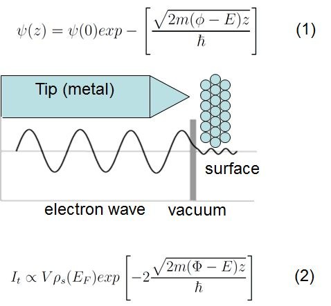
The Scanning Tunneling Microscopy (STM) was developed in 1984 and is based on the quantum mechanical tunneling effect enabling electrons to pass a non-conductive barrier. This effect occurs if the barrier width is so small that the exponentially decreasing wave function of the electrons on one side of the barrier (equation (1)) does not completely vanish on the other side, resulting in a finite probability for the electron to “tunnel” through this barrier to the other side. If a voltage is applied between both sides a closed circuit results, whose of current It depends exponentially on the barrier width and the distance of the two conducting sides respectively (equation (2)).
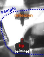
One side of the barrier described above is typically represented by the sample, the other side is represented by a conducting tip (usually made of tungsten or platinium-iridium). If this tip is brought into tunnel contact (distance ~0.1 nm) and raster-scanned over the sample, a vertical profile results from the course of the tunneling current. On the left side the actual sample setup is depicted: By eye, the tungsten tip is brought up from below towards the sample that is hanging overhead. Then a computer-controlled fine approach of the tip is performed until it is only some tenths of nanometers away from the sample. During the following raster-scanning the tunnel current is usually kept at a constant value (~0.01-1 nA) by means of a feedback loop. The scanner of our Omicron STM allows scan ranges of up to 18 x 18 µm2.
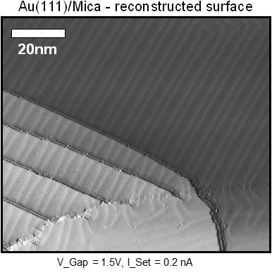
By raster scanning the surface of a (conducting) substrate, surface properties like atomic arrangements can be probed subsequently. As an example is given below the image of a gold surface with monatomic steps and the wave shaped reconstruction of the (111)-surface is depicted. The step height is 0.2 nm.
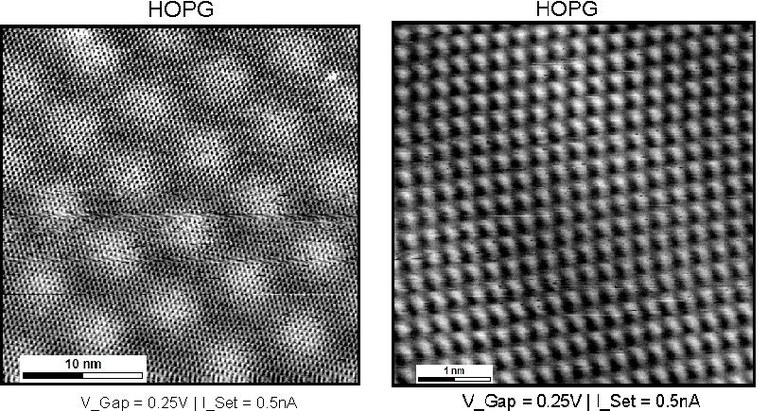
With sufficiently good tip quality and pureness of the sample atomic resolution can be achieved on some substrates at room temperature, as is the case with HOPG. In the left image the Moiré superstructure is clearly visible.
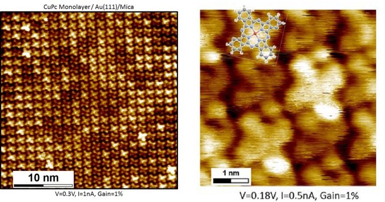
Adsorbed monolayers of organic molecules are also easily resolved on metal surfaces, for example copper-phthalocyanine on Au(111). Single molecules can be identified as shown by the inset in the right image.