Main Content
Core facility Semiconductor Epitaxy
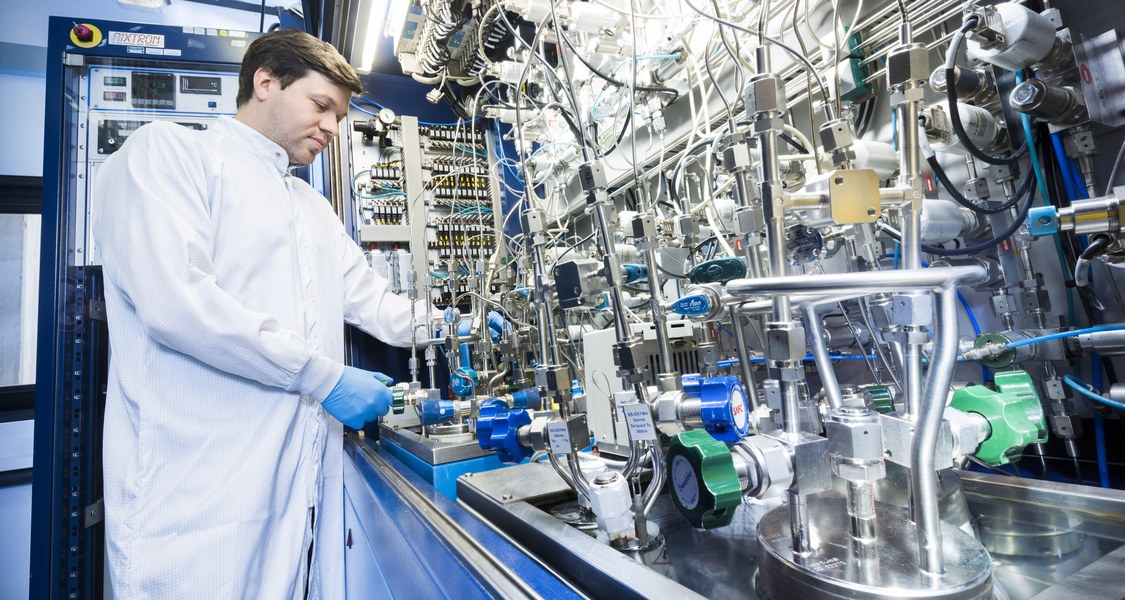
Ein Mitarbeiter arbeitet am MOVPE Reaktor
The terms of use for the semiconductor epitaxy as well as the hints for the user costs are listed under the following links:
Terms of use (PDF) (German)
Hinweise zu Gerätenutzungskosten und zu Gerätezentren (PDF)
Reactors for metal-organic vapor phase epitaxy (MOCVD) and atomic layer deposition (ALD)
| Device | Special characteristics | Location | person (Details S.b.) |
|---|---|---|---|
| 2 x 300mm Crius Cluster (Aixtron AG) |
III/V and SiGeC Epitaxie: Wafer size: up to 12" (300 mm), CVD machine: Si/Ge/C-epitaxy, MOVPE machine: III/V-epitaxy, Brooks wafer handler for loading and transfer of substrates, Epi Curve TT (LayTec) |
LB, mar.quest | SR, JZ, KV |
| JEOL JEM-Z200FSC (CRYO ARM™ 200) |
Two AIX 200 machines linked by Nitrogen filled glove-box: Equipped with EpiRAS (Laytec), Equipped with mass spectrometer (Zeiss), Materials: SiGeC, III/V and 2D (e.g. post-transition metal chalcogenides) |
LB, mar.quest | SR, JZ, KV |
| OXTRON | Home-built (MOVPE/CVD) machine: 2 hot sources for low-vapor pressure sources |
LB, mar.quest | SR, JZ, KV |
Characterization of semiconductors
| Device | Special characteristics | Location | person (Details S.B.) |
|---|---|---|---|
| Atomic force microscopy (AFM) | LB, mar.quest | ||
| X-ray diffraction (XRD) | LB, mar.quest | ||
| Photoluminescence (PL) | LB, mar.quest | ||
| Raman Spectroscopy | LB, mar.quest | ||
| ECV measurements | LB, mar.quest | ||
| Magnetotransport/Hall | LB, mar.quest |
Contact
| Name | Contact |
|---|---|
| C. Becker CB |
Tel.: 06421 / 28-22260 E-Mail: celina.becker@physik |
| Dr. A. Beyer AB |
Tel.: 06421 / 28-25704 E-Mail: andreas.beyer@physik |
| M. Hellwig MH |
Tel.: 06421 / 28-23458 E-Mail: michael.hellwig@staff |
| Stefan Reinhard SR |
Tel.: 06421 / 28-25691 E-Mail: stefan.reinhard@physik |
| Johannes Zimmet JZ |
Tel.: 06421 / 28-25691 E-Mail: johannes.zimmet@staff |
| Prof. Dr. K. Volz KV |
Tel.: 06421 / 28-22297 E-Mail: kerstin.volz@physik |
To complete an email address please add the following string ".uni-marburg.de".