Main Content
Core facility Semiconductor Epitaxy
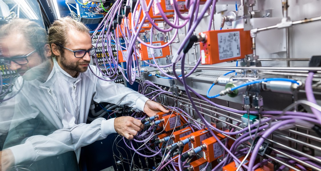
Reactors for metal-organic vapor phase epitaxy (MOCVD) and atomic layer deposition (ALD)
| Device | Special characteristics | Location | person (Details S.b.) |
|---|---|---|---|
| 2 x 300mm Crius Cluster (Aixtron AG) |
III/V and SiGeC Epitaxie: Wafer size: up to 12" (300 mm), CVD machine: Si/Ge/C-epitaxy, MOVPE machine: III/V-epitaxy, Brooks wafer handler for loading and transfer of substrates, Epi Curve TT (LayTec) |
LB, mar.quest | SR, JZ, KV |
| JEOL JEM-Z200FSC (CRYO ARM™ 200) |
Two AIX 200 machines linked by Nitrogen filled glove-box: Equipped with EpiRAS (Laytec), Equipped with mass spectrometer (Zeiss), Materials: SiGeC, III/V and 2D (e.g. post-transition metal chalcogenides) |
LB, mar.quest | SR, JZ, KV |
| OXTRON | Home-built (MOVPE/CVD) machine: 2 hot sources for low-vapor pressure sources |
LB, mar.quest | SR, JZ, KV |
Characterization of semiconductors
| Device | Special characteristics | Location | person (Details S.B.) |
|---|---|---|---|
| Atomic force microscopy (AFM) | LB, mar.quest | ||
| X-ray diffraction (XRD) | LB, mar.quest | ||
| Photoluminescence (PL) | LB, mar.quest | ||
| Raman Spectroscopy | LB, mar.quest | ||
| ECV measurements | LB, mar.quest | ||
| Magnetotransport/Hall | LB, mar.quest |
Contact
| Name | Contact |
|---|---|
| C. Becker CB |
Tel.: 06421 / 28-22260 E-Mail: celina.becker@physik |
| Dr. A. Beyer AB |
Tel.: 06421 / 28-25704 E-Mail: andreas.beyer@physik |
| M. Hellwig MH |
Tel.: 06421 / 28-23458 E-Mail: michael.hellwig@staff |
| Stefan Reinhard SR |
Tel.: 06421 / 28-25691 E-Mail: stefan.reinhard@physik |
| Johannes Zimmet JZ |
Tel.: 06421 / 28-25691 E-Mail: johannes.zimmet@staff |
| Prof. Dr. K. Volz KV |
Tel.: 06421 / 28-22297 E-Mail: kerstin.volz@physik |
To complete an email address please add the following string ".uni-marburg.de".