Main Content
Quantum Materials
2D Materials
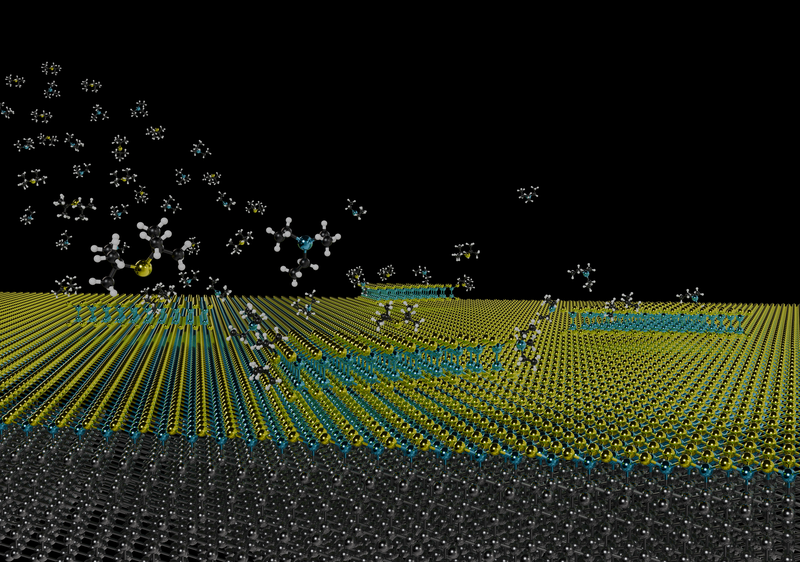
Since the fabrication of a free-standing graphene sheet—that is, the exfoliation of a single layer of carbon atoms—many researchers have been investigating graphene and other two-dimensional (2D) materials that are only a few atomic layers thick. These materials could enable the development of a new generation of technologies. Research in this field focuses on the synthesis of these materials as well as the study of their properties and stability. The focus of our research group is primarily on semiconducting 2D materials. We grow III–VI materials such as GaS or GaSe using metal-organic chemical vapor deposition (MOCVD) in advanced reactor systems and characterize their optoelectronic properties. In addition, we employ our high-performance electron microscopes for high-resolution imaging and spectroscopy to investigate the influence of structural defects on the material properties.
Nano-structured Semiconductors
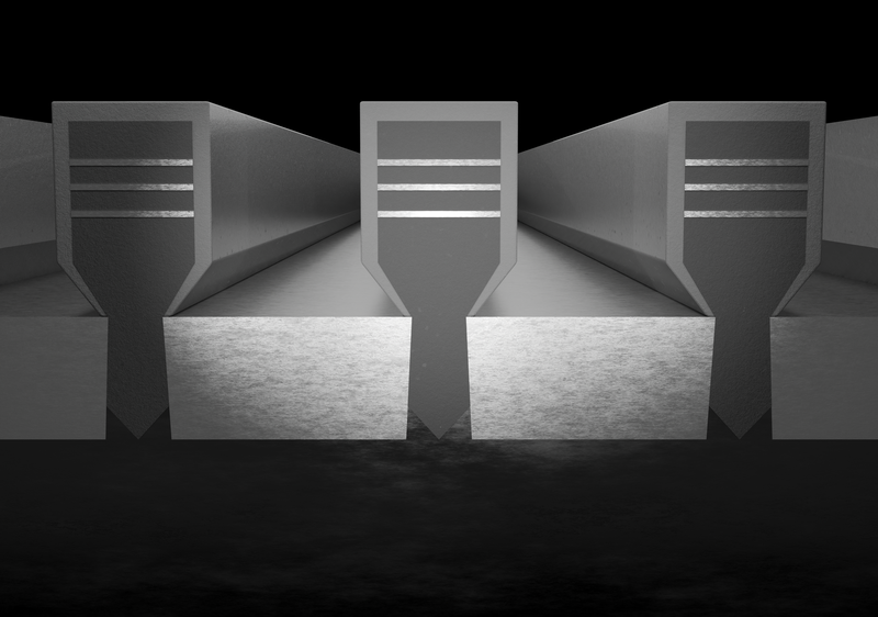
Optical data transmission using modern fiber-optic technology has now replaced electrical signal transmission in many areas. It is characterized by higher data rates and lower energy consumption. However, these advantages are not limited to large-scale applications; they can also be implemented in an integrated manner on small silicon chips. For high energy efficiency, light with a wavelength in the near-infrared range of around 1300 nm is optimal. In our research group, we therefore work on the fabrication of lasers with structural dimensions in the nanometer range, so-called nanoridge lasers, using semiconductor materials that can emit light in this wavelength region. Our focus is on the direct growth of these laser structures by metal-organic vapor phase epitaxy (MOVPE), a method that enables the fabrication of complex crystalline thin films.