Hauptinhalt
2020
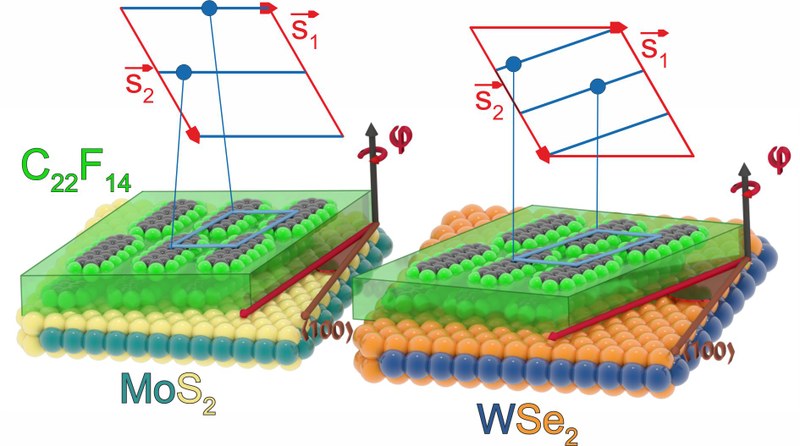
CHEM. MATER.: "Van der Waals Bound Organic Semiconductor/2D-Material HybridHeterosystems: Intrinsic Epitaxial Alignment of PerfluoropentaceneFilms on Transition Metal Dichalcogenides"
Maximilian Dreher, Darius Günder, Steffen Zörb and Gregor Witte
ACS Chem. Mater., 32, 20, 9034–9043 (2020), •Doi:
https://doi.org/10.1021/acs.chemmater.0c03482
Hybrid systems consisting of transition metal dichalcogenides (TMDCs) and organic semiconductors (OSCs) are promising candidates for future optoelectronic device architectures, as they combine the outstanding charge transport properties of TMDCs with the high photoabsorption cross-section and the ability to tailor the energy levels of OSCs through synthetic means. Since crystalline organic layers have very anisotropic optical absorption and emission characteristics, their azimuthal alignment is an important parameter for the efficiency of the optical coupling in such hybrid systems. The lack of dangling bonds makes surfaces of 2D materials quite inert and smooth and therefore allows an unrestricted growth of organic adlayers without the requirement of relaxation or commensurability at the interface, which is an important prerequisite for van der Waals (vdW) epitaxy. Here, we have studied the formation and azimuthal alignment of crystalline adlayers of the OSC perfluoropentacene (PFP) on the basal plane of MoSe2, WSe2, MoS2, and MoTe2 single crystals representing the most ideal TMDC surfaces, which are further compared with corresponding films on graphene and hBN. Combining specular X-ray reflectivity with polarization resolved optical reflection measurements allowed the azimuthal alignment of crystalline PFP domains to be precisely analyzed, which revealed characteristic twist angles between adlayer and substrate lattices for the various 2D materials. This orientational order can be rationalized as an on-line coincidence and is well reproduced by model calculations that are based on the scheme of projection of real-space adlayer lattice points onto the substrate unit cell. The extreme sensitivity of the resulting rotational alignment of epitaxial adlayers on the smallest changes of the lattice parameters is demonstrated by distinctly different twist angles for PFP films that were grown at an elevated temperature and thus show a slight thermal expansion. The presently introduced and validated model to describe the epitaxial alignment in weakly bound crystalline adlayers can also be applied to other vdW bound heterosystems and can be useful to elucidate the peculiarities of vdW epitaxy.ACS APPL. MATER. INTERFACES: "Van der Waals bound Organic/2D-Insulator Hybrid-Structures: Epitaxial Growth of Acene Films on hBN(001) and the Influence of Surface Defects "
Darius Guender, Kenji Watanabe, Takashi Taniguchi, and Gregor Witte
ACS Appl. Mater. Interfaces, 12, 38757 - 38767 (2020). •Doi: https://doi.org/10.1021/acsami.0c09527
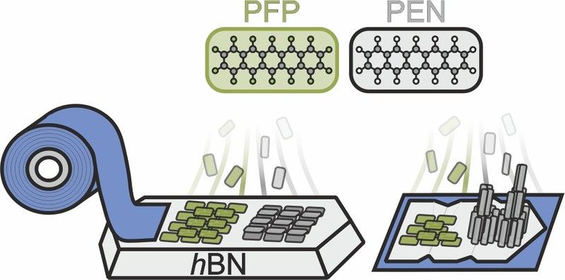
Combining 2D materials with functional molecular films enables the fabrication of van der Waals bound organic/inorganic hy-brids that are of interest for future device architecture. Recently, the 2D dielectric hexagonal boron nitride (hBN) has received par-ticular attention, since exfoliation allows the preparation of crystalline layers which have been utilized as ultrathin dielectrics in electronic devices. Here, we have studied the formation and structure of molecular films of the prototypical organic semiconduc-tors pentacene (PEN) and perfluoropentacene (PFP) on hBN. Special attention was paid to the influence of substrate surface de-fects on the film formation by comparing molecular films that were grown on hBN substrates of various quality, including single crystals (representing the most ideal surface), briefly ion bombarded substrates and exfoliated flakes. While X-ray diffraction (XRD) yields precise information on the crystalline structure of films grown on (large) single crystals, it is hardly applicable to analyze the films formed on exfoliated flakes because of their small size. Here, we demonstrate that in the case of flakes, detailed structural analyses of the molecular films are possible by combining atomic force microscopy (AFM) with micro-spot UV/Vis-spectroscopy and optical polarization microscopy. On well-ordered hBN single crystal surfaces both acenes form very smooth and epitaxial crystalline films where molecules adopt a recumbent orientation (even in 100nm thick films). By contrast, both materials adopt an upright molecular orientation and different polymorphs on defective hBN surfaces and reveal distinctly different film morphologies. On exfoliated flakes, PFP shows a film structure similar to that on the hBN single crystals, while PEN films exhibit a structure as on defective hBN substrates. In addition, a pronounced decoration of defect steps, which are probably created by the exfoliation process, was observed for PEN leading to the formation of tall and extended fibers where molecules adopt a recumbent orientation. The present study reveals different robustness in film growth on exfoliated hBN flakes for various molecules, which has to be considered in their device integration, especially with regard to their optoelectronic properties such as light absorption or charge transport, which depend critically on the molecular orientation and crystalline order.J. PHYS. CHEM. C: "Evolution of TiOPc Films on Au(111): from Seed Layer to Crystalline Multilayers"
Felix Widdascheck, Michael Kothe, Sebastian Thussing, Peter Jakob, Gregor Witte
J. Phys. Chem. C, 124, 27, 14664-14671 (2020, •Doi:
https://doi.org/10.1021/acs.jpcc.0c03244
Since optoelectronic properties of organic semiconductor films are closely linked to their structural properties (such as molecular orientation, crystalline phase and orientation, degree of crystallinity etc.), a microscopic understanding of hetero-growth behavior is of utmost importance to control and improve such films for device applications. For the case of titanyl phthalocyanine (TiOPc), a widely used molecular semiconductor for organic optoelectronics, the initial film growth on metal substrates has already been studied extensively by means of scanning tunneling microscopy (STM), whereas the molecular arrangement in seed layers and the subsequent film growth are controversially discussed. Here, we combined scanning probe microscopy [(STM) and atomic force microscopy (AFM)] with X-ray diffraction (XRD) and reflection absorption infrared spectroscopy (RAIRS) to shed some light on this debate and analyzed the evolution of TiOPc films on Au(111) ranging from initial seed layers up to thick multilayers (50nm) aiming at preparing long-range ordered films and identifying their structure. We demonstrate that long range ordered films are formed at 450K, where molecules reveal an all oxygen-up orientation in the monolayer and an oxygen-down geometry in the second layer, while ruling out phases comprising inclined molecules based on corresponding RAIRS data. Such bilayers are stabilized by the oppositely oriented axial dipole moments forming stable building blocks that cause a subsequent bilayer-wise growth, yielding very smooth multilayers which exclusively crystallize in the phase I polymorph, hence parallels the growth scenario observed before for Ag(111) substrates. Films prepared at room temperature exhibit reduced ordering and the appearance of several metastable phases, none of them involving inclined molecules. The present study emphasizes the importance of using complementary techniques to obtain a compre-hensive picture of organic film growth, while an analysis based solely on imaging techniques can sometimes lead to incorrect conclusions.ANG. CHEMIE: "Unilaterally Fluorinated Acenes: Synthesis and Solid State Properties"
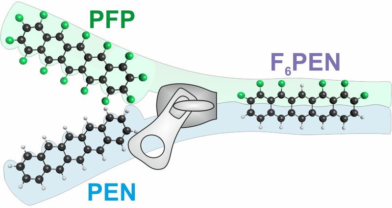
Philipp E. Hofmann, Matthias W. Tripp, Daniel Bischof, Yvonne Grell, Anna L. C. Schiller, Tobias Breuer, Sergei I. Ivlev, Gregor Witte, Ulrich Koert
Angewandte Chemie, 59, 16501 - 16505 (2020) •Doi: https://doi.org/10.1002/anie.202006489
The rapid development of organic electronics is closely related to the availability of molecular materials with specific elec‐tronic properties. Here, we introduce a novel synthetic route enabling a unilateral functionalization of acenes along their long side, which is demonstrated by the synthesis of 1,2,10,11,12,14‐hexafluoropentacene ( 1 ) and the related 1,2,9,10,11‐pentafluorotetracene ( 2 ). Quantum chemical DFT calculations in combination with optical and X‐ray absorption spectroscopy data indicate that the single molecular properties of 1 are a connecting link between the organic semiconductor model systems pentacene (PEN) and perfluoropentacene (PFP). In contrast, the crystal structure analysis reveals a different packing motif than for the parental molecules, which can be related to distinct F…H interactions identified in the corresponding Hirshfeld surface analysis and also affects solid state properties such as the exciton binding energy and the sublimation enthalpy.LANGMUIR: "Chemical Surface Reactivity and Morphological Changes of Bismuth Triiodide (BiI3) under Different Environmental Conditions"
Bettina Wagner, Andrea Huttner, Daniel Bischof, Annikka Engel, Gregor Witte and Johanna Heine
Langmuir, 36, 6458-6464 (2020) •Doi: https://doi.org/10.1021/acs.langmuir.0c00740
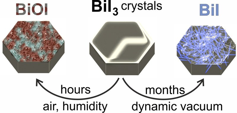
Layered metal halides like BiI3 are of current interest both in connection with 2D materials and photovoltaics. Here, we present a facile new method for the preparation of millimeter-sized BiI3 single crystals. We use these crystals to study the surface reactivity of their (001) cleavage planes towards various environmental conditions by measuring morphological changes using atomic force microscopy and analysing the formed species by means of X-ray photoelectron spectroscopy and X-ray diffraction methods. We find that freshly cleaved samples show atomically flat surface regions extending over several μm and reveal steps corresponding to single BiI3 layers. However, we also find that the surface deteriorates in air on a time-scale of hours. By studying samples cleaved and stored under different conditions, we identify water as the agent initiating the changes in surface morphology, while under inert gas and dry oxygen, the surface stays intact. Based on the analysis of deteriorated long-term stored samples we identify BiOI as the main product of hydrolysis. We also observe a second long-term decomposition route for samples stored under dynamic vacuum, where the formation of BiI whiskers occurs. Overall, our findings emphasize the challenges associated with the surface reactivity of BiI3, but also demonstrate that well-ordered BiI3 surfaces can be obtained, which indicates that a preparation of extended, atomically smooth BiI3 monolayers by exfoliation from bulk crystals should be possible.APPL. SURF. SCI.: "The Effect of Oxygen Plasma Treatment of Gold Electrodes on the Molecular Orientation of CuPc Films"
Felix Widdascheck Felix Widdascheck, Michael Kothe, Alrun A. Hauke and Gregor Witte
Appl. Surf. Sci., 507, 145039 (2020) • DOI: 10.1016/j.apsusc.2019.145039
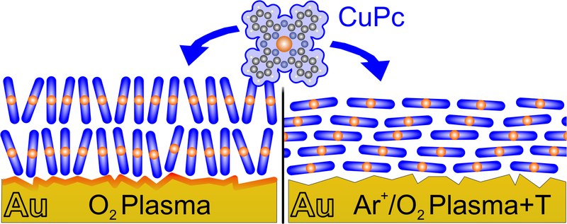
Gold (Au) is a commonly used material for many organic electronic device electrodes due to its chemical stability and high work function, which is required for p-type semiconductors. The orientation and morphology of organic semiconductors deposited on such electrodes often depends crucially on the cleanliness of the Au surface. In this study, we examine the effect of a common cleaning method, namely oxygen plasma cleaning, on sputter-deposited polycrystalline Au electrodes and subsequently deposited copper-(II)-phthalocyanine (CuPc) films. Using X-ray diffraction (XRD), atomic force microscopy (AFM) and near-edge X-ray absorption fine structure (NEXAFS) measurements, we show that the metastable Au oxide typically formed during an oxygen plasma cleaning process significantly impacts the molecular orientation and morphology in CuPc thin films, forcing molecules to adopt an upright orientation. We further demonstrate that the typical recumbent orientation of CuPc adopted on clean polycrystalline Au can be achieved by an additional annealing step after oxygen plasma treatment of the Au electrode that causes a decomposition of the gold oxide.