Hauptinhalt
2021
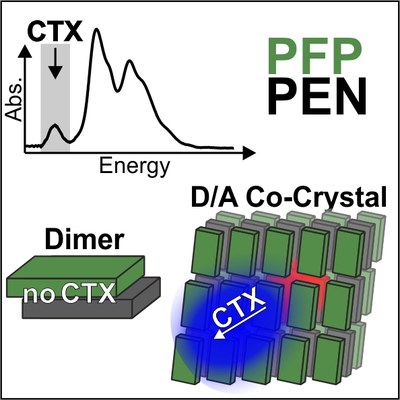
J. PHYS. CHEM. LETT.: "Polarization Resolved Optical Excitation of Charge-Transfer Excitons in PEN: PFP Cocrystalline Films: Limits of Nonperiodic Modeling"
Darius Günder, Ana M. Valencia, Michele Guerrini, Tobias Breuer, Caterina Cocchi
and Gregor Witte
J. Phys. Chem. Lett., 12, 9899−9905 (2021), •Doi: 10.1021/acs.jpclett.1c02761
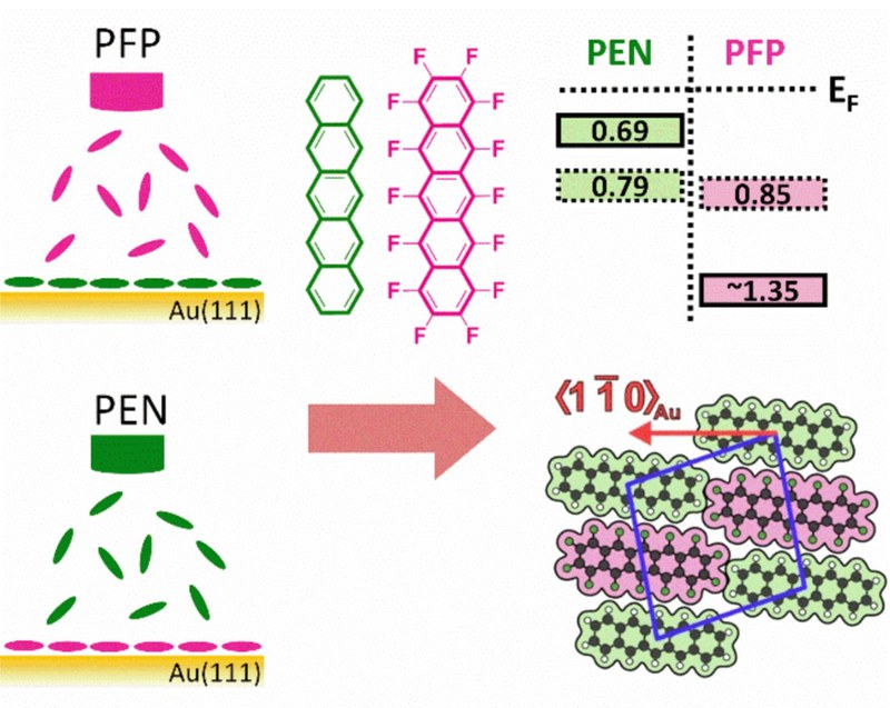
Charge-transfer excitons (CTXs) at organic donor/acceptor interfaces are considered important intermediates for charge separation in photovoltaic devices. Crystalline model systems provide microscopic insights into the nature of such states as they enable microscopic structure−property investigations. Here, we use angular-resolved UV/vis absorption spectroscopy to characterize the CTXs of crystalline pentacene:perfluoro-pentacene (PEN:PFP) films allowing determination of the polarization of this state. This analysis is complemented by first-principles many-body calculations, performed on the three-dimensional PEN:PFP cocrystal, which confirm that the lowest-energy excitation is a CTX. Analogous simulations performed on
bimolecular clusters are unable to reproduce this state. We ascribe this failure to the lack of longrange interactions and wave function periodicity in these cluster calculations, which appear to remain a valid tool for modeling properties of organic materials ruled by local intermolecular
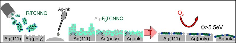
couplings.ADV. FUNCT. MATER.: "Engineering of Printable and Air-Stable Silver Electrodes with High Work Function using Contact Primer Layer: From Organometallic Interphases to Sharp Interfaces"
Felix Widdascheck, Daniel Bischof, Gregor Witte
Adv. Funct. Mater., 202106687(2021), •Doi:
10.1002/adfm.202106687
Contact engineering is an important issue for organic electronics as it allows to reduce charge carrier injection barriers. While the use of molecular contact primer layers to control the energy level alignment is demonstrated in many concept studies, mainly using (single crystalline) model substrates, the processability of electrodes and their robustness must also be considered in real devices. Although silver electrodes can be printed using silver ink, their low work function and sensitivity to oxidation severely limits their use for printable organic electronics. The present study demonstrates that monolayers of F4TCNQ and F6TCNNQ provide a reliable approach to engineer high work function silver electrodes, which is examined for Ag(111) as well as polycrystalline and silver ink substrates. Notably, upon multilayer growth, a pronounced intercalation of silver into the molecular adlayer occurs, yielding thermally stabilized organometallic interphases extending over the entire adlayer. It is shown that heating allows their controlled desorption leaving behind a well-defined monolayer that is further stabilized by additional charge transfer. Especially F6TCNNQ contact primer layers can also be prepared on oxidized silver electrodes yielding work functions of 5.5–5.6 eV, which can even withstand air exposure. Such contact primers show no interdiffusion into subsequently deposited layers of the prototypical p-type organic semiconductor pentacene, hence validating their use for organic electronic devices.J. PHYS. CHEM. C.: "Perfluorinated Acenes: Crystalline Phases, Polymorph-Selective Growth, and Optoelectronic Properties"
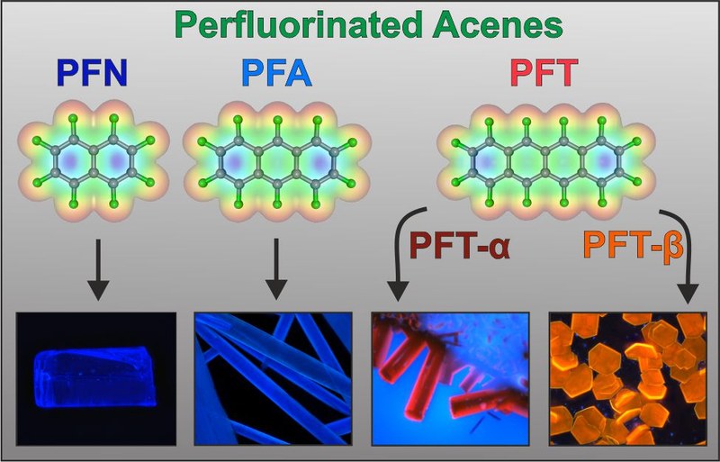
Daniel Bischof, Marc Zeplichal, Sebastian Anhäuser, Akshai Kumar, Martin Kind, Franziska Kramer, Michael Bolte, Sergei I. Ivlev, Andreas Terfort, and Gregor Witte
J. Phys. Chem. C., 125, 34, 19000–19012 (2021), •Doi: 10.1021/acs.jpcc.1c05985
The emerging field of organic electronics triggers the search for new molecular semiconductors and fluorophores. Since optoelectronic properties of molecular solids also depend crucially on molecular packing motifs, it is not sufficient to only consider single-molecule properties, but also to gain precise knowledge of the crystalline phases to understand structure–property relationships. Here, we analyze and compare structural and optoelectronic properties of perfluorinated acenes ranging from perfluoronaphthalene (PFN) via perfluoroanthracene (PFA) and perfluorotetracene (PFT) to perfluoropentacene (PFP), while previous studies, due to the lack of availability of PFA and PFT, were limited to PFN and PFP, which exhibit rather different crystal structures. Applying various crystallization techniques such as gradient sublimation, solution growth, and liquid-assisted organic molecular beam deposition, we identified different crystalline phases that allow closing this structural gap. A comparison of all known phases reveals clear trends in the molecular packing motifs, which are rationalized by corresponding Hirshfeld analyses. Using UV/vis and X-ray absorption spectroscopy, also optoelectronic solid state properties of the various compounds were analyzed, and from a comparison with the corresponding solution spectra, the exciton binding energies are estimated. In addition, we demonstrate that like PFP PFT also exhibits a π-stacked polymorph in films grown on graphene, where molecules are flat lying and adopt a slip-stacked packing. This interface-mediated phase is found to be stable only for PFP and PFT, while it is unstable for the smaller PFA. Finally, we demonstrate for the case of PFT that the different packing motifs occurring in the various phases have a strong influence on the photoluminescence spectra.Nanoscale: "Temperature-Programmed Desorption of Large Molecules: Influence of Thin Film Structure and Origin of Intermolecular Repulsion"
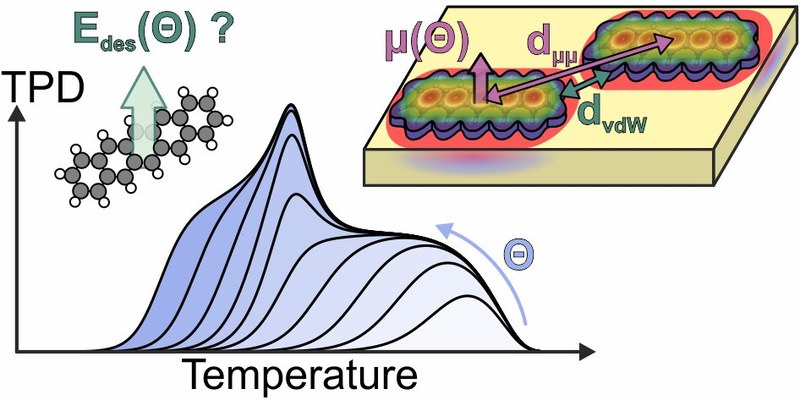
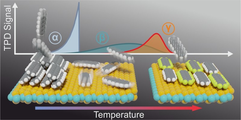
Pierre-Martin Dombrowski, Stefan Renato Kachel, Leonard Neuhaus, J. Michael Gottfried and Gregor Witte
Nanoscale, 13, 13816-13826 (2021), •Doi: 10.1039/D1NR03532K
Although the exact knowledge of the binding energy of organic adsorbates on solid surfaces is of vital importance for the realization of molecular nanostructures and the theoretical modelling of molecule-substrate interactions, an experimental determination is by no means trivial. Temperature-programmed desorption (TPD) is a widely used technique that can provide such information, but a quantitative analysis requires detailed knowledge of the pre-exponential factor of desorption and is therefore rarely performed on a quantitative level for larger molecules that often exhibit notable mutual intermolecular interactions. Here, we provide a thorough anlysis of TPD data of monolayers of pentacene and perfluoropentacene adsorbed on Au(111) that serve as a model system for polycyclic aromatic hydrocarbons adsorbed on noble metal surfaces. We show that the pre-exponential factor varies by several oders of magnitude with the surface coverage and evolves in a step-like fashion due to the sudden activation of a rotational degree of freedom during thermally controlled monolayer desorption. Using complementary coverage-dependent work function measurements, the interface dipole moments were determined. This allows to identify the origin and quantify the relative contributions of the lateral intermolecular interactions, which we modelled by force field calculations. This analysis clearly shows that the main cause for intermolecular repulsion are electrostatic interactions between the intramolecular charge distributions, while interface dipoles play only a minor role.Nanoscale Adv.: "Pentacene/perfluoropentacene bilayers on Au(111) and Cu(111): impact of organic–metal coupling strength on molecular structure formation†"
Qi Wang, Jiacheng Yang, Antoni Franco-Cañellas, Christoph Bürker, Jens Niederhausen, Pierre Dombrowski, Felix Widdascheck, Tobias Breuer, Gregor Witte, Alexander Gerlach, Steffen Duhm and Frank Schreiber
Nanoscale Adv., 3, 2598 - 2606 (2021), •Doi: 10.1039/d1na00040c
As crucial element in organic opto-electronic devices, heterostructures are of pivotal importance. In this context, a comprehensive study of the properties on a simplified model system of a donor-acceptor (D-A) bilayer structure is presented, using ultraviolet photoelectron spectroscopy (UPS), X-ray photoelectron spectroscopy (XPS), low-energy electron diffraction (LEED) and normal-incidence X-ray standing wave (NIXSW) measurements. Pentacene (PEN) as donor and perfluoropentacene (PFP) as acceptor material are chosen to produce bilayer structures on Au(111) and Cu(111) by sequential monolayer deposition of the two materials. By comparing the adsorption behavior of PEN/PFP bilayers on such weakly and strongly interacting substrates, it is found that: i) the adsorption distance of the first layer (PEN or PFP) indicates physisorption on Au(111), ii) the characteristics of the bilayer structure on Au(111) are (almost) independent of the deposition sequence, and hence, iii) in both cases a mixed bilayer is formed on the Au substrate. This is in striking contrast to PFP/PEN bilayers on Cu(111), where strong chemisorption pins PEN molecules to the metal surface and no intermixing is induced by subsequent PFP deposition. The results illustrate the strong tendency of PEN and PFP molecules to mix, which has important implications for the fabrication of PEN/PFP heterojunctions.ACS APPL. MATER. INTERFACES: "Charge Transfer Excitation and Asymmetric Energy Transfer at the Interface of Pentacene−Perfluoropentacene Heterostacks"
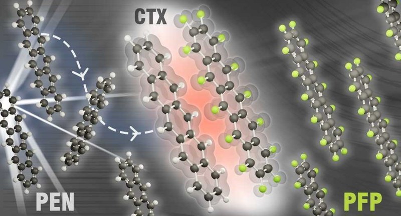
Anna-Katharina Hansmann, Robin C. Döring, Andre Rinn, Steffen M. Giesen, Melanie Fey, Tobias Breuer, Robert Berger, Gregor Witte, and Sangam Chatterjee
Appl. Mater Interfaces,13, 5284 - 5292 (2021) •Doi: 10.1021/acsami.0c16172
High-performance solar cells demand efficient charge-carrier excitation, separation, and extraction. These requirements hold particularly true for molecular photovoltaics, where large exciton binding energies render charge separation challenging at their commonly complex donor–acceptor interface structure. Among others, charge-transfer (CT) states are considered to be important precursors for exciton dissociation and charge separation. However, the general nature of CT excitons and their formation pathways remain unclear. Layered quasiplanar crystalline molecular heterostructures of the prototypical donor–acceptor system pentacene–perfluoropentacene studied at cryogenic temperatures are a paramount model system to gain insights into the underlying physical mechanism. In particular, a detailed experiment–theory analysis on a layered heterojunction featuring perfluoropentacene in its π-stacked polymorph and pentacene in the Siegrist phase indicates that exciton diffusion in unitary films can influence the formation efficiency of CT excitons localized at internal interfaces for these conditions. The correlation of the structural characteristics, that is, the molecular arrangement at the interfaces, with their absorption and photoluminescence excitation spectra is consistent with exciton transfer from pentacene to the CT exciton state only, whereas no transfer of excitons from the perfluoropentacene is detected. Electronic structure calculations of the model systems and investigation of coupling matrix elements between the various electronic states involved suggest hampered exciton diffusion toward the internal interface in the perfluoropentacene films. The asymmetric energy landscape around an idealized internal donor–acceptor interface thus is identified as a reason for asymmetric energy transfer. Thus, long-range effects apparently can influence charge separation in crystalline molecular heterostructures, similar to band gap bowing, which is well established for inorganic pn-junctions.APPL. ELECTRON. MATER.: "B3N3‑Substituted Nanographene Molecules: Influence of Planarityon the Electronic Structure and Molecular Orientation in Thin Films"
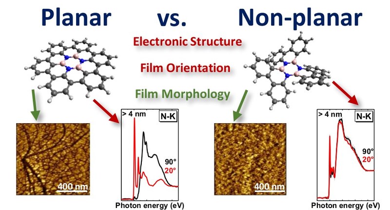
Katharina Greulich, Axel Belser, Daniel Bischof, Felix Widdascheck, Marie S. Sättele, Peter Grüninger, Holger F. Bettinger, Gregor Witte, Thomas Chassé, and Heiko Peisert
APPL. ELECTRON. MATER, 3, 825-837 (2021), •Doi: 10.1021/acsaelm.0c00967
BN-substituted nanographene molecules are currently the focus of interest because the substitution of C–C units by isoelectronic and isosteric BN units is a straightforward way of changing the electronic properties of nanographenes. Another parameter influencing the electronic structure, orientation, and growth mode of nanographene molecules is the planarity of the molecules. The electronic structure, orientation, and film growth of the related molecules B3N3-hexa-peri-hexabenzocoronene (BN-HBC), B3N3-hexabenzotriphenylen (BN-HBP), and B3N3-hexabenzotriphenylen-2H (BN-HBP-2H) on Au(111) have been studied by photoelectron spectroscopy (PES), X-ray absorption spectroscopy (XAS), atomic force microscopy (AFM), and scanning tunneling microscopy (STM). XA spectra were simulated using time-dependent density functional theory (TDDFT). The calculation of C 1s excitation spectra allows the assignment of individual transitions and the examination of the degree of cross-linking between biphenyl units. It is shown that the planarity of the molecules distinctly affects the electronic structure, interface properties a well as growth in thin films.PCCP: "Selective Saturation of Step-Edges as a Tool to Control the Growth of Molecular Fibres"
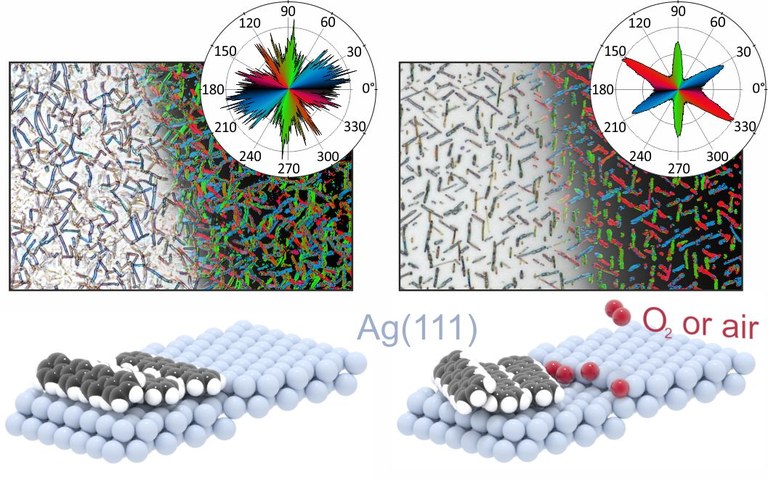
Maximilian Dreher and Gregor Witte
PCCP, 23, 8023-8029 (2021) •Doi: 10.1039/D0CP06725C
The concept of bottom-up self-organisation has become a promising alternative for structuring molecular materials, which is hardly accessible by conventional top-down approaches such as lithography due to their limited chemical robustness. While these materials often tend to form three-dimensional, crystalline islands or fibres upon film growth, the size and orientation of such fibres are mainly governed by appropriate preparation conditions as well as microscopic interactions at the interface with the supporting surface. Substrate surface defects such as vacancies or step-edges, which cannot be completely ruled out on real surfaces on the mesoscopic scale, can act as prefered nucleation sites for molecules that leads to parasitic film growth competing with their intrinsic alignment prevailing on an ideal surface. In the present study we demonstrate for the case of para-quaterphenyl (p-4P), that the presence of azimuthally disordered, fibres on Ag(111) surfaces can be understood as a superposition of step-mediated nucleation and the intrinsic epitaxial fibre growth on ideal surfaces. We validate the concept by purposely exposing the silver substrates briefly to oxygen or even ambient air to passivate the more reactive step-sites, which hampers subsequenty grown molecular films to nucleate at these step-edges. This yields a truly epitaxial alignment as well as an enlargement of the fibres present on the whole sample.EURJOC: "Synthesis and Molecular Properties of Partially Fluorinated DNTTs"
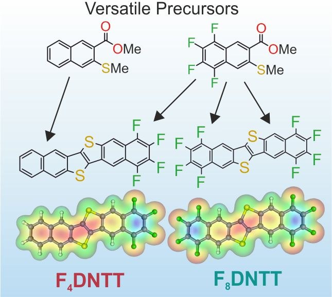
Matthias W. Tripp, Daniel Bischof, Maximilian Dreher, Gregor Witte, and Ulrich Koert
EurJOC, 1295-1304 (2021) •Doi: 10.1002/ejoc.202001635
1,2,3,4-Tetrafluoro-dinaphtothienothiophene (F4DNTT)
and 1,2,3,4,8,9,10,11-octafluoro-dinaphtothienothiophene (F8DNTT)
were synthesized via bisthiomethyl alkene intermediates which were
accessible by McMurry coupling or Wittig olefination of partially
fluorinated naphthalene precursors. DFT-based electronic structure
calculations, near edge X-ray absorption fine structure (NEXAFS)
spectroscopy and UV/Vis measurements were used for
HOMO/LUMO gap determination and to analyze the electronic
structures of the partially fluorinated DNTTs. Reduced exciton binding was observed in thin films.CHEM SCI: "Engineering of TMDC–OSC hybrid interfaces: the thermodynamics of unitary and mixed acene monolayers on MoS2"
Stefan R. Kachel, Pierre-Martin Dombrowski, Tobias Breuer, J. Michael Gottfried and Gregor Witte
CHEM SCI, 12, 2575–2585 (2021) •Doi: 10.1039/d0sc05633b
Hybrid systems of two-dimensional (2D) materials such as transition metal dichalcogenides (TMDCs) and organic semiconductors (OSCs) have become subject of great interest for future device architectures. Although OSC–TMDC hybrid systems have been used in first device demonstrations, the precise preparation of ultra-thin OSC films on TMDCs has not been addressed. Due to the weak van der Waals interaction between TMDCs and OSCs, this requires precise knowledge of the thermodynamics at hand. Here, we use temperature-programmed desorption (TPD) and Monte Carlo (MC) simulations of TPD traces to characterize the desorption kinetics of pentacene (PEN) and perfluoropentacene (PFP) on MoS2 as a model system for OSCs on TMDCs. We show that the monolayers of PEN and PFP are thermally stabilized compared to their multilayers, which allows preparation of nominal monolayers by selective desorption of multilayers. This stabilization is, however, caused by entropy due to a high molecular mobility rather than an enhanced molecule–substrate bond. Consequently, the nominal monolayers are not densely packed films. Molecular mobility can be suppressed in mixed monolayers of PEN and PFP that, due to intermolecular attraction, form highly ordered films as shown by scanning tunneling microscopy. Although this reduces the entropic stabilization, the intermolecular attraction further stabilizes mixed films.OrgEl: "Prepare with care: Low contact resistance of pentacene Field-Effect transistors with clean and oxidized gold electrodes"
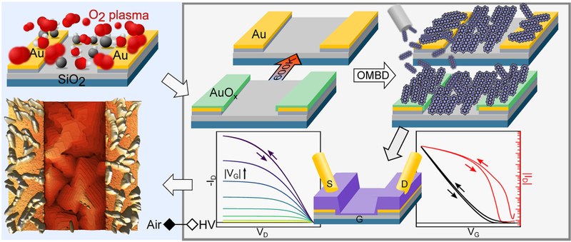
Yurii Radiev, Felix Widdascheck, Michael Göbel, Alrun Aline Hauke, Gregor Witte
OrgEl, 89, 106030 (2021) •Doi: 10.1016/j.orgel.2020.106030
In recent years, a number of researchers have voiced concerns regarding the increasing amount of publications which report record performance characteristics of organic field-effect transistors (OFETs). These devices often make use of elaborate architectures, ranging from surface treatment by self-assembled monolayers to contact-limited doping, injection layer introduction etc. While these techniques are claimed to improve the device performance, they often result in poorly defined device interfaces, such as that of the organic semiconductor with the dielectric and electrode surfaces, which render a rigorous theoretical description of the interface effects close to impossible. Furthermore, the effects of ambient exposure of prepared devices are often neglected during the analysis. In this work we introduce a completely high vacuum-based manufacturing and electrical characterization of OFETs using commercially available gold bottom-contact bottom-gate FET structures, which enables a rigorous exclusion of any air contact of the devices. Using the example of the prototypical and widely studied organic semiconductor pentacene, we compare various initial cleaning procedures of the FET-structures prior to the vacuum deposition of pentacene films on the device characteristics and complement the electrical in situ analysis by ex situ AFM measurements of the pentacene film morphology. We demonstrate that O2 plasma cleaning with subsequent thermal annealing under vacuum conditions results in well-defined interfaces of the pentacene film with clean surface of gold electrodes, which exhibit a remarkably low width-normalized contact resistance of 1.19 kΩcm. Additionally, we show that the formation of gold oxide on top of the electrodes as a result of O2 plasma cleaning without subsequent heating is beneficial for the charge carrier injection, resulting in a contact resistance of only 0.16 kΩcm – to the best of our knowledge, one of the lowest yet reported values for pentacene-gold systems. In addition, the comparative rigorous vacuum-based processing and analysis allows in particular to study also the effects of controlled exposure to ambient air – even for a short time – as well as aging under different storage conditions on the device performance.MATER. CHEM. C: "Stability of organic thin-film transistors based on ultrathin films of dinaphtho[2,3-b:2’,3’f]thieno[3,2-b]thiophene (DNTT)"
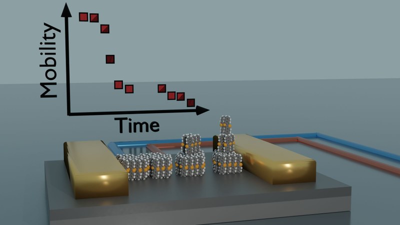
Rachana Acharya, Darius Günder, Tobias Breuer, Guido Schmitz, Hagen Klauk and Gregor Witte
J. Mater. Chem. C, 9, 270-280 (2021), •Doi: 10.1039/D0TC04554C
Organic thin-film transistors (TFTs) based on ultrathin semiconductor films are potentially useful as highly sensitive physical, chemical or biological sensors and may also help in the development of a better understanding of the relations between structural and charge-transport characteristics in thin films of organic semiconductors. A particularly promising small-molecule organic semiconductor is dinaphtho[2,3-b:2’,3’-f]thieno[3,2-b]thiophene (DNTT). However, it was recently reported that ultrathin DNTT films spontaneously undergo dramatic morphological changes within minutes after deposition that lead to the disaggregation of the initially closed (or at least connected) single-monolayer films into disconnected multilayer islands. Here, we investigate how this spontaneous structural reconfiguration affects the characteristics of TFTs based on ultrathin DNTT films and explore the extent to which it can be prevented by cryogenic cooling or in-situ encapsulation. We fabricated inverted coplanar TFTs with a hybrid aluminum oxide / alkylphosphonic acid self-assembled monolayer gate dielectric and vacuum-deposited DNTT films with nominal thicknesses of 2.5 or 25 nm. Using atomic force microscopy (AFM) we monitored the spontaneous changes in the DNTT morphology in a quasi-continuous manner over a period of 12 hours after deposition. The charge-carrier mobility of the ultrathin DNTT TFTs was found to decrease rapidly, while the mobility of the TFTs with the thicker DNTT films is far more stable. We also found that the initial closed-monolayer morphology of the ultrathin DNTT films is preserved when the substrates are cooled to cryogenic temperatures immediately after the DNTT deposition, but that the morphological changes resume upon returning the substrates to room temperature. Furthermore, we fabricated TFTs in which the ultrathin DNTT films were encapsulated in-situ with a vacuum-deposited film of polytetrafluoroethylene, C60 or titanyl phthalocyanine immediately following the DNTT deposition and found that the encapsulation decelerates the structural reorganization of the ultrathin DNTT films and the concurrent degradation of the carrier mobility.