Hauptinhalt
2025
EURJIC: A Family of Luminescent Halido Cadmates with BifunctionalDiammonium Cations
M. Yang, R. O. Kusche, S. Anhäuser, J. Möbs, G. Witte,
and J. Heine
EURJIC, 28, e202500264 (2025), • DOI: 10.1002/ejic.202500264
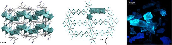
Two different-sized diammonium cations yield a family of luminescent halido cadmates, including a chlorido cadmate featuring a novel anion motif and a low-temperature phase transition based on a conformation change in the organic cation, with relevance to phase transition engineering in 2D lead.Adv. Mater.: Unveiling the Effects of Hydroxyl-Induced Trap States on the Charge Transport in p- and n-Channel Organic Field-Effect Transistors through Variable-Temperature Characterization

Y. Radiev, T. Wollandt, H. Klauk, and G. Witte
Adv. Mater., 2505631 (2025), • DOI: 10.1002/adma.202505631
Trap states at the gate dielectric-organic semiconductor (OSC) interface are one of the main sources of extrinsic traps in organic field-effect transistors (OFETs). However, they are often overlooked and their effects on the charge transport are attributed to the exposure of devices to ambient air. Here a first variable-temperature transfer length method characterization of both p- and n-channel OFETs under full high vacuum conditions is reported. By comparing a hydroxylated aluminum oxide (Al2O3) gate dielectric with a hydroxyl-free, tetradecylphosphonic acid-functionalized Al2O3 dielectric, it is shown that hydroxyl-induced trap states reduce the charge carrier mobility in OFETs regardless of the channel type. This observation challenges the common belief that the hydroxyl-induced traps are affecting primarily the n-channel transport. The variable-temperature analysis yields a high activation energy of charge transport as the main effect of a hydroxylated gate dielectric. Moreover, the injection barrier at the interface between the source-drain electrodes and the OSC layer is significantly lower for devices with a hydroxyl-free dielectric and correlates with the activation energy of charge transport. This work identifies previously hidden limitations of charge transport in OFETs, opening opportunities for further improvements in device performance and potential device applications.ACS Nano: Reliability of the Transmission Line Method and Reproducibility of the Measured Contact Resistance of Organic Thin-Film Transistors
T. Wollandt, S. Steffens, Y. Radiev, F. Letzkus, J. N. Burghartz, G. Witte, H. Klauk
ACS Nano, 19, 10, 9915–9924 (2025), • DOI: 10.1021/acsnano.4c15828
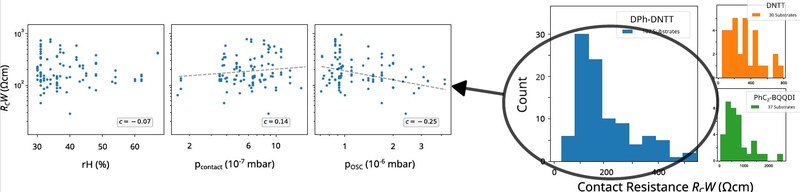
Using the transmission line method (TLM), we extracted the contact resistance of organic thin-film transistors (TFTs) based on five different vacuum-deposited small-molecule semiconductors fabricated on over 500 substrates. In the first part of this report, we illustrate how the reliability of the TLM analysis is affected by the statistical uncertainty that arises from the fitting procedure and by the systematic error that is introduced if the actual channel length of the TFTs deviates from the nominal channel length. In the second part, we show that the contact resistance of organic TFTs varies significantly from one fabrication run to the next (and even across substrates fabricated within the same fabrication run), no matter how much care is taken to keep all controllable fabrication-process parameters constant. A statistical analysis reveals no strong correlations between the contact resistance and environmental parameters present during TFT fabrication, such as the humidity in the laboratory or the base pressure of the vacuum during material depositions. This suggests that the observed variation in the contact resistance is mainly stochastic. For the TFTs based on the best-performing semiconductor, the contact resistance varies between 28 Ωcm and 1 kΩcm, with a median value of 160 Ωcm.