Hauptinhalt
2026
Adv. Funct. Mater.: Beyond the Edge: Charge-Transfer Excitons in Organic Donor-Acceptor Cocrystals
S. Anhäuser, A. M. Valencia, S. I. Ivlev, M. Zeplichal, A. Terfort, C. Cocchi, G. Witte
ADFM, 30499 (2026), • DOI: 10.1002/adfm.202530499
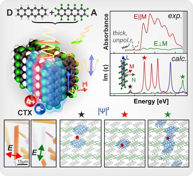
Charge-transfer excitons (CTXs) at organic donor/acceptor interfaces are crucial intermediates for charge separation in photovoltaic devices. While blends used in real-world devices hamper detailed characterization of CTXs, atomistic models of cocrystals offer powerful alternatives for gaining microscopic insights. In this work, we investigate electronic and optical properties of acene-perfluoroacene cocrystals (anthracene, tetracene, and pentacene), combining experimental synthesis and characterization with first-principles calculations based on many-body theory. We prepare ultrathin cocrystals for polarization-resolved transmission-absorption spectroscopy, linking exciton polarization with molecular packing. Complementing this analysis, density-functional and many-body perturbation theory reveal complex excitonic landscapes that challenge several common assumptions about CTXs in weakly interacting donor-acceptor systems. For the studied cocrystals, we demonstrate that such CTXs are not limited to the absorption onset, but also occur at higher energy and produce sharp, intense absorption features. Adopting the intrinsic molecular coordinate system, we categorize the various excitons according to their polarization and show that the transition dipole moment of the lowest energy CTX is not necessarily aligned with the donor-acceptor stacking axis. We further characterize triplet excitons from first principles, which are only indirectly accessible experimentally. This work provides a deep understanding of CTXs in organic cocrystals, developing a refined conceptual framework that is crucial for future design of environmentally sustainable photoactive materials.SMALL: Low Temperature MOCVD Synthesis of High-Mobility 2D InSe
R. Günkel, O. Maßmeyer, M. Stein, K. Bräumer, R. Sandoval Rodriguez, D. Anders, J.-H. Littmann, S. Anhäuser, B. Ojaghi Dogahe,M. Bergmann, M. Solanki, N. F. Langlotz, J. Glowatzki, J. Belz, A. Beyer, G. Witte, S. Chatterjee, K. Volz
Smll, 10911 (2026), • DOI: 10.1002/smll.202510911
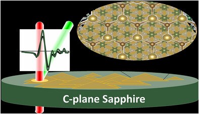
2D indium selenide (InSe) is a layered semiconductor with high electron mobility and a tunable band gap ranging from 1.25 eV in the bulk to 2.8 eV in the monolayer limit. However, growing phase-pure InSe remains challenging due to the complex indium–selenium (In–Se) phase diagram. This complexity and the sensitivity of chemical precursors to growth conditions make it difficult to control which In–Se phase forms during synthesis during, e.g., metal-organic chemical vapor deposition (MOCVD). MOCVD is considered the most promising approach for growing InSe, as it enables wafer-scale, uniform, and controllable deposition—key requirements for device integration. We present a systematic investigation of InSe synthesis on c-plane sapphire substrates at low temperatures. By varying Se/In precursor ratio and growth temperature, we create a phase diagram that covers In-rich, equal stoichiometric, and Se-rich InxSey phases. Raman spectroscopy and atomic force microscopy, supported by energy dispersive X-ray spectroscopy and scanning transmission electron microscopy, reveal formation conditions of 2D InSe. The epitaxial alignment is verified by in-plane X-ray diffraction. Samples grown under optimized conditions exhibit a strong optical absorption in the visible range and especially a comparably high electron mobility, underlining the potential of the MOCVD-grown material for future applications.